QUOTE(SSJBen @ Jul 27 2015, 03:23 PM)
Yup.
And remember all the claims they made about Kepler before launch... lol, many of which is untrue other than the "state-the-obvious" remarks.

It makes sense, 50-60% is quite similar to that of Kepler from Fermi and Maxwel from Kepler. HBM while interesting, I don't think we will see most of its potential until 2017, when DX12 and Vulkan is much more matured. NVLink apparently will be focused for supercomputers only, not sure if it will make it to the consumer grade cards or not? There's no confirmation on this.
Yeah, there is a rumor circulating around that PK100 will make the scenes first, instead of PK104. I honestly... doubt it?

ooo i'll google that up then.
then this nvlink ? sounds like not only do i buy the pascal gpu, but also need a new motherboard with nvlink as well ?
they say it would look this basically
QUOTE
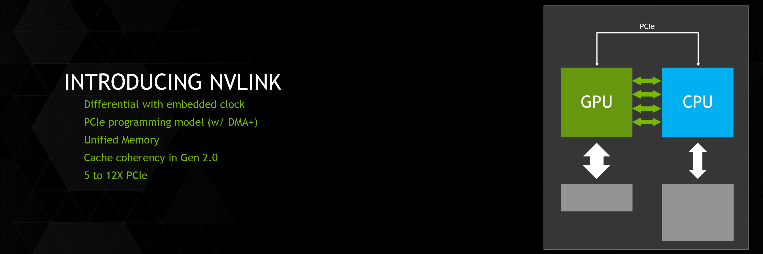
Coming to the final pillar then, we have a brand new feature being introduced for Pascal: NVLink. NVLink, in a nutshell, is NVIDIA’s effort to supplant PCI-Express with a faster interconnect bus. From the perspective of NVIDIA, who is looking at what it would take to allow compute workloads to better scale across multiple GPUs, the 16GB/sec made available by PCI-Express 3.0 is hardly adequate. Especially when compared to the 250GB/sec+ of memory bandwidth available within a single card. PCIe 4.0 in turn will eventually bring higher bandwidth yet, but this still is not enough. As such NVIDIA is pursuing their own bus to achieve the kind of bandwidth they desire.
The end result is a bus that looks a whole heck of a lot like PCIe, and is even programmed like PCIe, but operates with tighter requirements and a true point-to-point design. NVLink uses differential signaling (like PCIe), with the smallest unit of connectivity being a “block.” A block contains 8 lanes, each rated for 20Gbps, for a combined bandwidth of 20GB/sec. In terms of transfers per second this puts NVLink at roughly 20 gigatransfers/second, as compared to an already staggering 8GT/sec for PCIe 3.0, indicating at just how high a frequency this bus is planned to run at.

QUOTE
Multiple blocks in turn can be teamed together to provide additional bandwidth between two devices, or those blocks can be used to connect to additional devices, with the number of bricks depending on the SKU. The actual bus is purely point-to-point – no root complex has been discussed – so we’d be looking at processors directly wired to each other instead of going through a discrete PCIe switch or the root complex built into a CPU. This makes NVLink very similar to AMD’s Hypertransport, or Intel’s Quick Path Interconnect (QPI). This includes the NUMA aspects of not necessarily having every processor connected to every other processor.
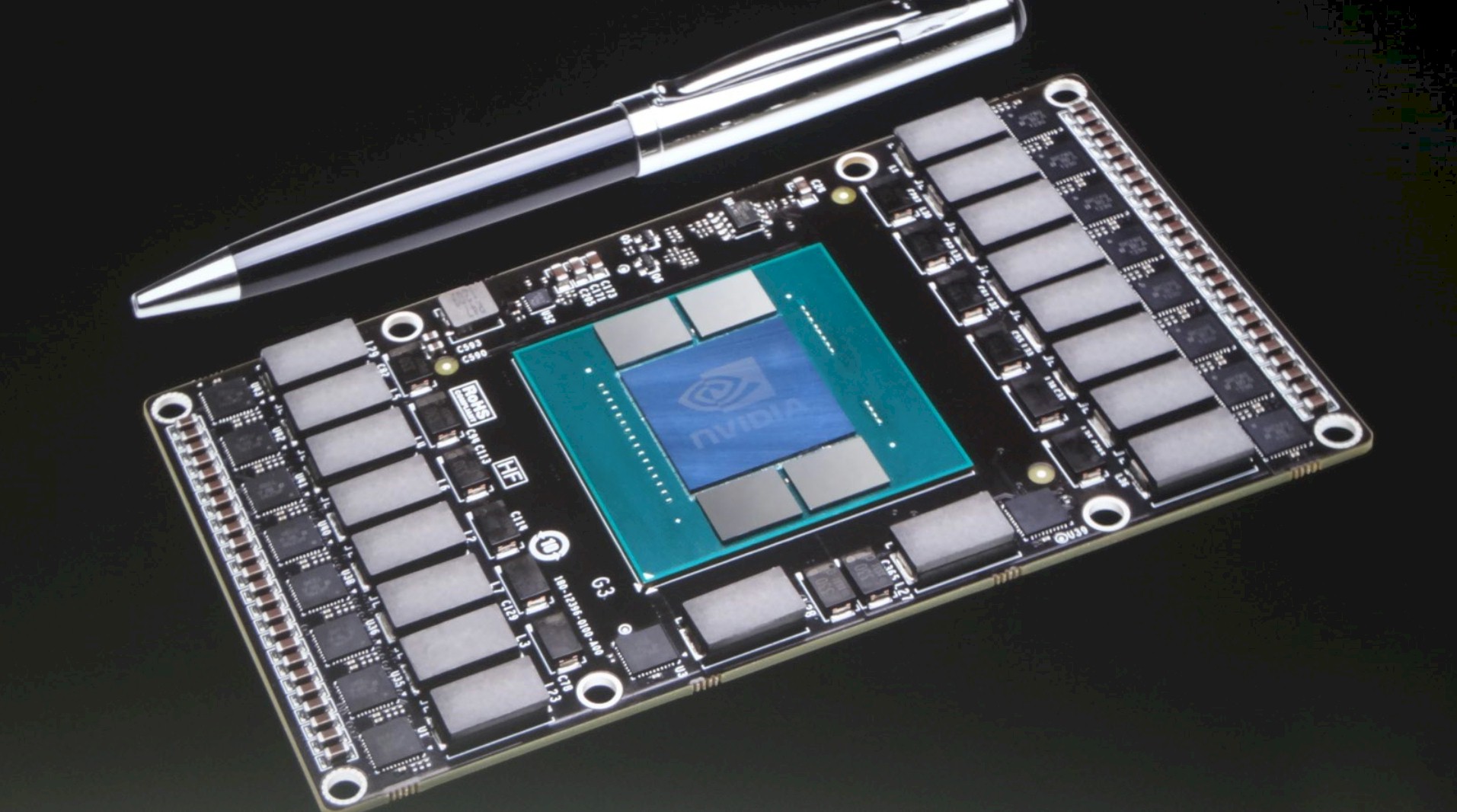
But the rabbit hole goes deeper. To pull off the kind of transfer rates NVIDIA wants to accomplish, the traditional PCI/PCIe style edge connector is no good; if nothing else the lengths that can be supported by such a fast bus are too short. So NVLink will be ditching the slot in favor of what NVIDIA is labeling a mezzanine connector, the type of connector typically used to sandwich multiple PCBs together (think GTX 295). We haven’t seen the connector yet, but it goes without saying that this requires a major change in motherboard designs for the boards that will support NVLink. The upside of this however is that with this change and the use of a true point-to-point bus, what NVIDIA is proposing is for all practical purposes a socketed GPU, just with the memory and power delivery circuitry on the GPU instead of on the motherboard.

Molex's NeoScale: An example of a modern, high bandwidth mezzanine connector
QUOTE
DIA is touting is that the new connector and bus will improve both energy efficiency and energy delivery. When it comes to energy efficiency NVIDIA is telling us that per byte, NVLink will be more efficient than PCIe – this being a legitimate concern when scaling up to many GPUs. At the same time the connector will be designed to provide far more than the 75W PCIe is spec’d for today, allowing the GPU to be directly powered via the connector, as opposed to requiring external PCIe power cables that clutter up designs.
With all of that said, while NVIDIA has grand plans for NVLink, it’s also clear that PCIe isn’t going to be completely replaced anytime soon on a large scale. NVIDIA will still support PCIe – in fact the blocks can talk PCIe or NVLink – and even in NVLink setups there are certain command and control communiques that must be sent through PCIe rather than NVLink. In other words, PCIe will still be supported across NVIDIA's product lines, with NVLink existing as a high performance alternative for the appropriate product lines. The best case scenario for NVLink right now is that it takes hold in servers, while workstations and consumers would continue to use PCIe as they do today.
Too much to quote, the rest is here
http://www.anandtech.com/show/7900/nvidia-...ecture-for-2016anyway sounds like nvlink mobo isn't a pre-requisite to use a pascal, can still use pcie. but the question, would using nvlink for a single gpu be worth it ? or is it only going to help for multi gpu setups ? I'm not a fan of multi gpus cause of driver support issues
so just wondering if upgrading to nvlink mobo is worth it for a single gpu setup. i rather wait for a cannonlake + before i upgrade
 This post has been edited by Moogle Stiltzkin: Jul 27 2015, 04:03 PM

 Jul 26 2015, 04:22 PM


 Quote
Quote
 regulating fan speeds with afterburner at the mean time.
 might need to get one soon.


 0.0319sec
 0.35
0.35
 6 queries
 GZIP Disabled