

 Mar 27 2013, 02:42 AM, updated 12y ago

*ARM Cortex Application Processors
(os) android, iOS, BB OS, Window Phone 8, Window RT
*Intel x86 processors; Atom processor family with a new system
on chip (SoC) platform designed for smartphones and tablets.
(os) android x86, Window 8(Full version)
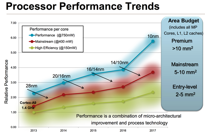
The Cortex A9 is too slow to compete with the likes of Intel’s Atom and Qualcomm’s Krait 200/300 based SoCs. The Cortex A15 on the other hand outperforms both of those solutions, but at considerably higher power and die area requirements.


http://www.arm.com/products/processors/cortex-a/index.php
QUOTE
ARM Cortex Application Processors
Cortex-A,

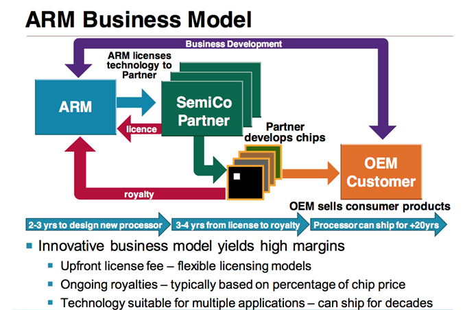
The ARM Diaries, Part 1: How ARM’s Business Model Works
http://www.anandtech.com/show/7112/the-arm...ess-model-works
ARMv7
http://en.wikipedia.org/wiki/ARM_architect...it_architecture
ARMv8
Cortex-A50 series, ARMv8-A future/To Be Announce SuperChip inside become (SuperPhone)

The Cortex-A50 Series is the latest range of processors based on the ARMv8 architecture. The series includes support for the AArch64, a new energy efficient 64-bit execution state that operates alongside an enhanced version of ARM’s existing 32-bit execution state. The Cortex-A50 Series comprises the Cortex-A57 and the Cortex-A53 processors.
These new low power processors will drive the widespread adoption of technology applications ranging from gesture control, augmented reality, mobile gaming, web 2.0 and entrepreneurial business applications, where data is the business.
Both the Cortex-A57 and Cortex-A53 processors can operate independently or be combined into an ARM big.LITTLE processing configuration that enables scalable performance and optimal energy-efficiency.
big.LITTLE
big.LITTLE is a heterogeneous computing architecture developed by ARM Holdings coupling slower, low-power processor cores with more powerful and power-hungry ones. The intention is to create a multi-core processor that can adjust better to dynamic computing needs and use less power than clock scaling alone. big.LITTLE was announced in October 2011 along with the Cortex-A7, which was designed to be architecturally compatible with the Cortex-A15. In October 2012 ARM announced the Cortex-A53 and Cortex-A57 ARMv8 cores, which are also compatible with each other to allow their use in a big.LITTLE chip.
more
http://en.wikipedia.org/wiki/Big.LITTLE
ARM Holdings itself does not manufacture its own electronic chips,
but licenses its designs to other semiconductor manufacturers.
ARM-based processors and systems on a chip include the:
Main stream
Snapdragon by Qualcomm; GPU Adreno
Qualcomm MSMxxxx by Qualcomm; GPU Adreno
NVIDIA Tegra by NVIDIA; GPU Ultra-low power(ULP) GeForce
OMAP by Texas Instruments; GPU PowerVR(under license)
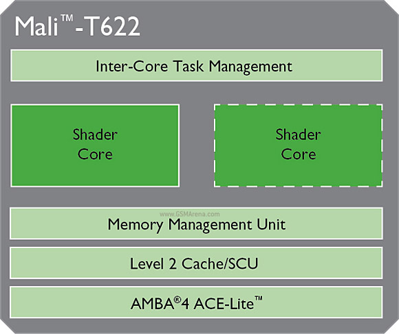
Exynos by Samsung; GPU Mali and PowerVR
NovaThor by ST-Ericsson; GPU Mali
[Hummingbird Core & Apple A4 by Samsung-Intrinsity]*not aviable for Android, Apple iDevice i(phone/pad/pod touch) only
[Ax by Apple (Common manufacturer Samsung Electronics)]*not aviable for Android, Apple iDevice i(phone/pad/pod touch) only
Other
K3V2 HiSilicon by Huawei
i.MX by Freescale Semiconductor (Spin-off from Motorola in 2004)
Axx by AllWinner
RK3xxx by Rockchip
BCMxxxx Broadcom
MTK MTxxxx by MediaTek
ARMxxxx by ARM Holdings (Common manufacturer OEM)
VIA WonderMedia PRIZM WMxxxx
Marvell Pantheon
Marvell ARMADA Mobile PXA986/PXA988
Marvell ARMADA Mobile PXA1088/1088 LTE
Renesas Mobile MP6530
TSMC (Taiwan Semiconductor Manufacturing Company)
GPU
http://en.wikipedia.org/wiki/PowerVR
http://en.wikipedia.org/wiki/Mali_(GPU)
http://en.wikipedia.org/wiki/Tegra
http://en.wikipedia.org/wiki/Adreno
http://en.wikipedia.org/wiki/Vivante_Corporation
Cortex-A,
The ARM Diaries, Part 1: How ARM’s Business Model Works
http://www.anandtech.com/show/7112/the-arm...ess-model-works
ARMv7
http://en.wikipedia.org/wiki/ARM_architect...it_architecture
| Cortex-A5 |
| Actions ATM702x | Atmel SAMA5D3 | Qualcomm Snapdragon 200/S4 Play | InfoTMIC iMAPx820 | iMAPx15 Telechips TCC892x |
| Cortex-A7 |
| Allwinner A2x, A3x | Leadcore LC1813 | MediaTek MT65xx | Qualcomm Snapdragon 200/400 | Samsung Exynos 5410 | Marvell PXA1088/1088 LTE |
| Cortex-A8 |
| Allwinner A1x | Apple A4 | Freescale i.MX5x | Rockchip RK291x | Samsung Exynos 3110/S5PC110/S5PV210 | Texas Instruments OMAP 3 | ZiiLABS ZMS-08 |
| Cortex-A9 |
| Actions ATMxxxx | Altera FPGAs | Amlogic AML8726 Apple A5/A5X | Freescale i.MX6x | HiSilicon K3V2 | Marvell PXA986/PXA988 | MediaTek MT657x | Nvidia Tegra 2/3/4i | Nufront NuSmart 2816M/NS115,/NS115M | Renesas EMMA EV2 | Rockchip RK292x/ RK30xx/RK31xx | Samsung Exynos 4 | ST-Ericsson NovaThor | Telechips TCC8803 | Texas Instruments OMAP 4 | VIA WonderMedia WM88x0/89x0 | Xilinx FPGAs | ZiiLABS ZMS-20/ZMS-40 |
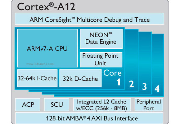
| Cortex-A12 |
| Rockchip RK3288 |
| Cortex-A15 |
| Allwinner A80 | Huawei HiSilicon K3V3 (big.LITTLE with dual-core Cortex-A7)(2+2) | MediaTek MT6599 | Nvidia Tegra 4/K1 (4+1 ARM Cortex A15) | Renesas Mobile MP6530 (big.LITTLE with dual-core Cortex-A7)(2+2) | Samsung Exynos 5 (big.LITTLE with quad-core Cortex-A7)(4+4) | Texas Instruments OMAP 5 |
| ARMv7-A compatible |
| Apple A6/A6X (Swift) | Broadcom Brahma-B15 | Marvell P4J | Qualcomm Snapdragon S1/S2/S3 (Scorpion) | Qualcomm Snapdragon S4 Plus/S4 Pro (Krait) |
| Qualcomm Snapdragon 600/800 (Krait 300/Krait 400) | Qualcomm Snapdragon 805 (Krait 450) |
ARMv8
Cortex-A50 series, ARMv8-A future/To Be Announce SuperChip inside become (SuperPhone)
QUOTE
The Cortex-A50 Series is the latest range of processors based on the ARMv8 architecture. The series includes support for the AArch64, a new energy efficient 64-bit execution state that operates alongside an enhanced version of ARM’s existing 32-bit execution state. The Cortex-A50 Series comprises the Cortex-A57 and the Cortex-A53 processors.
These new low power processors will drive the widespread adoption of technology applications ranging from gesture control, augmented reality, mobile gaming, web 2.0 and entrepreneurial business applications, where data is the business.
Both the Cortex-A57 and Cortex-A53 processors can operate independently or be combined into an ARM big.LITTLE processing configuration that enables scalable performance and optimal energy-efficiency.
| Cortex-A53 |
| Altera FPGAs | Qualcomm Snapdragon 410 |
| Cortex-A57 |
| ARM Cortex-A57 Processor on TSMC's 16nm FinFET Technology | AMD Hierofalcon |
| ARMv8-A compatible |
| Apple A7 (Cyclone) | Nvidia Tegra K1 (Project Denver) | Applied Micro Circuits Corporation | X-Gene |
big.LITTLE
big.LITTLE is a heterogeneous computing architecture developed by ARM Holdings coupling slower, low-power processor cores with more powerful and power-hungry ones. The intention is to create a multi-core processor that can adjust better to dynamic computing needs and use less power than clock scaling alone. big.LITTLE was announced in October 2011 along with the Cortex-A7, which was designed to be architecturally compatible with the Cortex-A15. In October 2012 ARM announced the Cortex-A53 and Cortex-A57 ARMv8 cores, which are also compatible with each other to allow their use in a big.LITTLE chip.
more
http://en.wikipedia.org/wiki/Big.LITTLE
ARM Holdings itself does not manufacture its own electronic chips,
but licenses its designs to other semiconductor manufacturers.
ARM-based processors and systems on a chip include the:
Main stream
Snapdragon by Qualcomm; GPU Adreno
Qualcomm MSMxxxx by Qualcomm; GPU Adreno
NVIDIA Tegra by NVIDIA; GPU Ultra-low power(ULP) GeForce
OMAP by Texas Instruments; GPU PowerVR(under license)
Exynos by Samsung; GPU Mali and PowerVR
NovaThor by ST-Ericsson; GPU Mali
[Hummingbird Core & Apple A4 by Samsung-Intrinsity]*not aviable for Android, Apple iDevice i(phone/pad/pod touch) only
[Ax by Apple (Common manufacturer Samsung Electronics)]*not aviable for Android, Apple iDevice i(phone/pad/pod touch) only
Other
K3V2 HiSilicon by Huawei
i.MX by Freescale Semiconductor (Spin-off from Motorola in 2004)
Axx by AllWinner
RK3xxx by Rockchip
BCMxxxx Broadcom
MTK MTxxxx by MediaTek
ARMxxxx by ARM Holdings (Common manufacturer OEM)
VIA WonderMedia PRIZM WMxxxx
Marvell Pantheon
Marvell ARMADA Mobile PXA986/PXA988
Marvell ARMADA Mobile PXA1088/1088 LTE
Renesas Mobile MP6530
TSMC (Taiwan Semiconductor Manufacturing Company)
GPU
http://en.wikipedia.org/wiki/PowerVR
http://en.wikipedia.org/wiki/Mali_(GPU)
http://en.wikipedia.org/wiki/Tegra
http://en.wikipedia.org/wiki/Adreno
http://en.wikipedia.org/wiki/Vivante_Corporation

QUOTE
Intel x86 processors
Atom by Intel
In 2012, Intel expanded the Atom processor family with a new system
on chip (SoC) platform designed for smartphones and tablets. It is
a continuation of the partnership announced by Intel and Google on 13
September 2011, to provide support for the Android operating system on
Intel x86 processors.
Atom SoC 2012
Atom Z2460 (codenamed Penwell; Medfield platform) Q2 2012
Atom Z2760 (codenamed Cloverview; Clover Trail platform) Q4 2012
Atom SoC 2013
Atom Z2420 (codenamed Lexington)
IntelAtomSoCAndroid-IA(X86)phone/tab,INTEL inside, SamsungGTab3/FHD-AsusFonepadNote6,MeMO10
https://forum.lowyat.net/topic/2752934
(For old era PDA Classic Processors)Atom by Intel
In 2012, Intel expanded the Atom processor family with a new system
on chip (SoC) platform designed for smartphones and tablets. It is
a continuation of the partnership announced by Intel and Google on 13
September 2011, to provide support for the Android operating system on
Intel x86 processors.
Atom SoC 2012
Atom Z2460 (codenamed Penwell; Medfield platform) Q2 2012
Atom Z2760 (codenamed Cloverview; Clover Trail platform) Q4 2012
Atom SoC 2013
Atom Z2420 (codenamed Lexington)
IntelAtomSoCAndroid-IA(X86)phone/tab,INTEL inside, SamsungGTab3/FHD-AsusFonepadNote6,MeMO10
https://forum.lowyat.net/topic/2752934
» Click to show Spoiler - click again to hide... «
This post has been edited by wkkm007: Feb 11 2014, 08:23 PM
 Quote
Quote


 0.0239sec
 0.83
0.83
 5 queries
 GZIP Disabled