QUOTE(ipohps3 @ Oct 16 2023, 09:56 PM)
doesn't matter
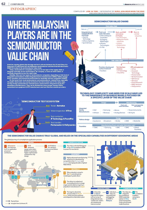
just want to say A&T is at the low end of the semicon value chain. just the quality checks for manufacturing.
the high value ones are R&D (POC, TR , EC, POR) for IP/SoC/IC design, integration, and verification at RTL and Gate level (ie from RTL to GDS II) and silicon wafer fabrication at foundry (also includes the standard cell library and PDK designs) . after these, are low value in the semicon industry chain.
Thanks for your sharing.
You worked in semiconductor industry very long time?
the most important and valuable steps in the semiconductor industry involve research and development (R&D) for designing and testing chips (IP/SoC/IC) at different stages, from the initial design (RTL) to the final product (GDS II), as well as making the physical silicon wafers in factories (foundries).
This also includes creating standard cell libraries and design kits. These early stages are where a lot of innovation happens and hold the most value.
After that, the later stages in the semiconductor manufacturing process are considered less valuable in the industry.
R&D: Research and Development - This is the process of creating and improving new technologies, products, or processes.
POC: Proof of Concept - It's a stage where you create a prototype to test whether your idea or technology is feasible.
TR: Technology Research - This involves studying and investigating new technologies or methods.
EC: Engineering and Design - This step includes the detailed design and engineering work for creating a product or technology.
POR: Product or Process Optimization - This phase is about refining and improving the final product or manufacturing process to make it as efficient and effective as possible.
RTL: RTL stands for Register-Transfer Level. It's an intermediate stage in integrated circuit (IC) design. At this stage, designers describe the behavior of the digital components in the IC using registers and the data transfers between them. RTL is closer to a human-readable description of the logic and functionality of the chip.
GDS II: GDS II (short for Graphic Data System II) is a file format used in semiconductor design and manufacturing.
It represents the final, highly detailed layout of all the components and interconnections on the silicon wafer. GDS II files are used to fabricate the actual physical semiconductor chip.
So, from RTL to GDS II represents the transition from a high-level, functional description of the chip (RTL) to the detailed layout and design that will be used to create the physical chip (GDS II).
It's a critical step in the semiconductor manufacturing process.


 Oct 16 2023, 11:20 AM, updated 3y ago


 Quote
Quote


 0.0289sec
 0.68
0.68
 5 queries
 GZIP Disabled