

 Feb 17 2008, 10:40 AM, updated 18y ago
My rig is down so I have some free time on my hands...... :-)
Note
1) My aim is to explain the complexity of a computer as simple as possible in simple English.
2) This guide is mainly in relation to overclocking.
3) I have no technical/electrical/computer training and I am not in any of these fields. Hence it is possible that my explanations may not be entirely correct (like a blind rat leading another!!!
 So, read at your own risk!!)
4) Any corrections/recommendations/advice are welcome (you can pm me)
5) I'm using Intel CPU Quad and gigabyte P35 motherboard as examples as I only have these parts
Index:
1) Part 1 : The basics
2) Part 2 : Those pesky BIOS settings that nobody understands....

3) Part 3 : In-depth explanation of essential BIOS settings
-------------------- Part 1 : The basics -----------------------
Make sure you know each of the important parts in a computer (see picture)
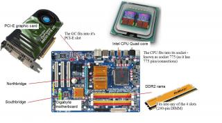
CPU - the brains of your computer
-Note : CPU is also used loosely to mean your whole computer including the casing (so don't get confused!)
- 2 major CPU giants are Intel and AMD
RAMs - the memory of your computer
Many types of desktop rams (from newest type):
- DDR3 rams (still expensive)
- DDR2 rams (currently the most used)
- DDR rams (going out of phase)
- SDrams (eh, still using it?
 )
)Graphic card - For display
Connects to many types of slots/interface
- PCI-E x16 slot (currently the best)
- AGP (older, going out of phase)
- PCI (eh, still available?
)Northbridge (NB) chipset
- act as a "bridge"
- important to connect and manage information between 4 parts of the computer - CPU, RAM, Graphic card and Southbridge
- also known as MCH (Memory Controller Hub) or GMCH (Graphics and MCH)
- examples of northbridge chipsets are P35, G33, nvidia 680 (other examples......)
In overclocking, the NB is a very important component. Hence, overclockers usually replace the stock heatsink with a better one.
Southbridge (NB)
- also act as a "bridge"
- important to connect and manage information from PCI cards, PCI-E x1, USB, Hard disk (SATA, IDE), Audio chipset, LAN chipset, SMBUS, etc....
- the southbridge communicates with the northbridge through the DMI (Direct Media Interface)
- examples of southbridge chipsets are ICH9, ICH8, etc....
Note : How to identify your NB/SB? In modern motherboards, the NB has a larger heatsink compared to the SB.
Note x2 : AMD rigs doesn't have a NB (explain later....)
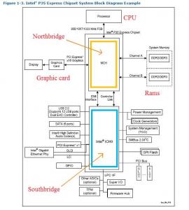
Front side bus (FSB) - also known as Host/processor/system bus
- the bus that connects the CPU and the northbridge
- the speed for the FSB can run at either 200/266/333 Mhz
- However, because each clock cycle can have 4 transfers, the resulting speed can be:
--- 800 MT/s (200mhz x 4 transfers)
--- 1066 MT/s (266mhz x 4 transfers)
--- 1333 MT/s (333mhz x 4 transfers)
- MT/s = Megatransfers for second (and because it is per second, it can be quoted in mhz!)
- Intel term this technique of 4 transfers per clock tick as "Quad Pumping"
Relations of the FSB to CPU speed
- The CPU speed is determined by 2 factors : FSB and CPU multiplier
- For example:
--- The Q6600 runs at 266mhz FSB x 9 CPU multiplier = 266 x 9 = 2.4Ghz
--- The E6750 runs at 333mhz FSB x 8 CPU multiplier = 333 x 8 = 2.66Ghz
- In overclocking, you can increase the CPU speed by either increasing the FSB or CPU multiplier
--- However, normal CPUs have their CPU multiplier "locked" at a certain limit e.g. Q6600 max at 9x, E6750 max at 8x
--- Due to this, increasing the FSB is the main method of overclocking
--- This does not apply to expensive extreme version of CPUs where their CPU multiplier are "unlocked"
Relations of the FSB to DDR2 rams
- Similarly, the DDR2 RAM speed is determined by 2 factors : FSB and RAM multiplier
- For example:
--- A DDR2-800 ram runs at 266mhz FSB x 3.0 RAM multiplier = 800mhz
--- It can also run at 333mhz FSB x 2.4 RAM multipler = 800mhz
Note : Just received my DFI Blood Iron motherboard..... will include the options of the RAMs in BIOS later.....
- In addition, DDR2 RAMs are capable of 2 transfers per clock cycle (hence the word "Double Data Rate (DDR))
Effect of increasing the FSB speed in overclocking
- So, as you will now realize, when you increase the FSB speed:
1) The communication between the CPU and NB is faster (which is an advantage!
 )
)2) Your CPU AND your RAM speed will also increase
3) Your northbridge has to work harder (hence more power consumption and heat generation) - that's why overclockers uses good 3rd-party NB coolers!!!
Here's a diagram of how these components are connected
If there is a FRONT side bus (FSB), is there such a thing as BACK side bus (BSB)???
- As a matter of fact, there is!!!!
- However, for modern PCs, you don't have to worry about this
- For completeness sake, the BSB is a computer bus used to connect the CPU to the CPU cache memory, usually L2.
- CPUs that have a back side (
 ) includes IBM PowerPC and Intel Pentium Pro.....
--------------------- Part 2 : Those pesky BIOS settings that nobody understands....
--------------------Disclaimer : I don't pretend I understand what I'm about to describe. What I have researched over the net, I'm just summarizing and making it easy to understand.
Voltage references mainly for P35 chipset.
So, examples of the dreaded settings are:
Voltages
- vMCH
- vFSB
- SB voltage
- NB core voltage
- CPU PLL voltage
- Clockgen voltage
- CPU GTL 0/2 Ref voltage (@ A/GTL ratio)
- CPU GTL 1/3 Ref voltage
- NB GTL ref voltage
- VTT FSB voltage @ FSB termination voltage
Others
- CPU voltage damper
- Loadline calibration
vMCH = Northbridge voltage
Default voltage : 1.3-1.4v (depends on your mobo)
Plays a critical role in overclocking. Important to maintain stability.
Higher voltage helps in overclocking the FSB @ making your rams run stable (if you're running 4 sticks of ram)
Important : Use active cooling on the NB. Advisable to have NB temperature less than 45'c to ensure stability
vFSB = VTT (termination voltage) = FSB termination voltage
Default voltage : 1.2V
Helps when at high FSB speeds
SB I/O Power = Southbridge voltage
Default voltage : 1.5V (for the ICH9R chipset)
Previously ignored during overclocking, however, increasing the voltage may sometimes improve the stability between NB and SB, and may help overclocking.
To be continued....
While the brute force approach will satisfy some users, those looking for a maximum stable overclock with the minimum amount of voltages will find GTL tuning a necessity.
vMCH = NB voltage = 1.4v default
vFSB = FSB termination voltage = VTT (Termination voltage) = 1.2v default
NB GTL ref voltage =
Coming up
In-depth explanation of essential BIOS settings
Basic
- Know that computers operate on a binary system, where information is communicated using "One"s and "Zero"s. e.g 010010111010000101111
- This is called binary logic or digital logic, where "1" represents the ON state and "0" represents the OFF state
- The ON and OFF state are achieved by using voltage levels know as logic levels (which commonly involves a range of voltage e.g. 0v and 5v)
- For example:
--- Anything between 3.5v-5.0v results in an ON state (or "ONE" @ 1)
--- Anything between 0v-1.5v results in an OFF state (or "ZERO" @ 0)
- If you understand the above, you will understand that to send some signals like "101" will involve changes in voltages like 4.0v then 0.8v then 4.2v.......
Follow so far?
Ok, now, know that the Front Side Bus (FSB) uses this type of signalling technology, the most advance up to now is the "Gunning Transceiver Logic (GTL)" which is superior to older signalling technology like CMOS, TTL, etc.
- Most Intel processor FSB signals use [Advanced] GTL (A/GTL)
Aha! So, this is the culprit GTL in the BIOS settings....... Interested? Read on....

This post has been edited by kmarc: Mar 21 2008, 02:12 PM
 Quote
Quote 0.0144sec
 0.78
0.78
 6 queries
 GZIP Disabled