

 Dec 13 2006, 10:59 PM, updated 19y ago
Dun mind the GRAFIC card spelling. weird as it seems, it sounds modern...

so, here it is
Comparison of Grafic Cards
In the following briefly we will list all grafic cards for Notebooks, which are available at the market. Additionally we represent approximate values of different bench marks (3D Mark at the moment) in italic style beneath the display adapters.
Performance class 1
They can be compared with current high end Desktop video cards of the impact of a X800 and 6800. The cards contain a similar core, however usually they are minor clocked and therefore somewhat more slowly. The newest games should run fluently with all details.
* 2x NVIDIA GeForce Go 7900 GTX SLI
2x GeForce video cards, which are combined by SLI on NVidia NForce 4 SLI Chipset
same specifications like 7900 GTX graphic card.
about 26.600 / 24.500 3DMark 01 / 03
* 2x NVIDIA GeForce Go 7900 GS SLI
2x GeForce video cards, which are combined by SLI on NVidia NForce 4 SLI Chipset
same specifications like 7900 GS video card.
about 24400 / 21800 3D Mark 01 / 03
* 2x NVidia Geforce Go 7800 GTX SLI
2x by SLI combined Geforce cards with NVidia NForce 4 SLI
specifications, Benchmarks: NBC News
> 10.000 3D Mark 05
* NVIDIA GeForce Go 7950 GTX
Successor of the GeForce Go 7900 GTX with higher clock speed and the same technical details. Current consumption should be similar like 7900 GTX.
* NVidia Geforce Go 7900 GTX
24 pixel-, 8 vertex-pipelines, 500 MHz Chip- and 1.200 MHz memory clock, 256 bit GDDR3-memory, Shader model 3.0, 45 Watts current consumption, max 512 MB VRAM; Benchmark: notebookreview.com (engl)
? / 18.200 / 8.500 / 4.700 3DMark 01 / 03 / 05 / 06
* ATI Mobility Radeon X1900 (rumour, no infos yet published)
codename M59, R580 architecture
according to Inquirer a little bit faster and hotter than X1800
* NVidia Geforce Go 7900 GS
20 Pixel-, 7 vertex-pipelines, 375 MHz Chip- and 1000 MHz memory clock, 256 bit GDDR3-memory, max 256 MB VRAM
23600 / 14000 / 6300 / 3800 3DMark 01 / 03 / 05 / 06
* ATI Mobility Radeon X1800XT
16 pixel-pipelines, 256 bit memory bus, Shader 3.0, codename M58, R520 architecture, probably up to 550 MHz core- and 650 memory clock, benchmark: X1800XT vs 7800GTX (engl)
about 7300? 3DMark 05 (6700 in 1280 resolution)
* NVidia GeForce Go 7800 GTX
24 pixel-, 6 vertex-pipelines, 400 MHz chip- and 1.100 MHz memory clock, 256 bit GDDR3-memory, Shader 3.0, pin-compatible to its predecessor (go 6800), codename G70M, 400 - 440 MHz core- and 500-550 MHz memory clock, practically the same current consumption / heat creation, like the 6800 Ultra
benchmark: notebookcheck.com, X1800XT vs 7800GTX (engl)
about 24800 / 14800 / 6600 3DMark 01 / 03 / 05
* ATI MOBILITY RADEON X800XT
16 pixel -, 6 vertexpipelines, 256 bit memory, PixelShader 2.0, code name M28Pro
about? / 22000/11000/5200 3DMark 01/03/05
* ATI Mobility Radeon X1800
12 pixel-pipelines, 256 bit memory-bus, shader 3.0, codename M58, R520 architecture, 450 MHz core- and 500 memory clock; about 5500 3DMark 05 according the first Vorserienmodell
* NVidia Geforce Go 7800
16 pixel-, 6 vertex-pipelines, 256 bit memory bus
about 19500 / 9300 / 3800 3DMark 01 / 03 / 05
* ATI MOBILITY RADEON X800
12 pixels -, 6 vertexpipelines, 128/256 bit memory, PixelShader 2.0, code name M28, bench mark: gamespot.com, anandtech.com
about 19100/8600 3DMark 01/03 (256 bits)
* Nvidia Geforce Go 6800 Ultra
12 pixels -, 5 vertexpipelines, 256 bit, high-clocked Geforce Go 6800, bench mark: anandtech.com, tomshardware.com
about 23800/11000 3DMark 01/03
* NVidia Geforce Go 6800
12 pixels -, 5 vertexpipelines, 128/256 bit, benchmark: gamespot.com, anandtech.com, tomshardware.com
about 20000/9500 3DMark 01/03 (256 bits)
* NVidia Quadro FX 2500M
256 bit memory bus, CAD optimized video card, up to 512MB video card, G71 architecture, 500 MHz core clock, 1200 MHz memory clock (DDR)
about ? / ? / 8400 / 4690 3DMark 01 / 03 / 05
* Nvidia Quadro FX 1500M
256 Bit memory bus, CAD optimized video card, up to 256MB graphics memory, G71 architecture, 7900GS based?
benchmark: Dell Precision M90
about 6400 / 3900 3DMark 05 / 06
* NVidia Quadro FX Go 1400
CAD version of Go 6800 (the usage of professional drivers is possible)
* ATI Mobility Radeon 9800
8 pixels -, 4 vertexpipelines, 256 bit, benchmark: Hardwareluxx.de, tomshardware.de,
tomshardware.com
about 17800/6500 3DMark 01/03
Performance class 2
Just as the performance class 1 these cards are comparable with video cards for desktop computers with the same name. The newest games should run with all details fluently.
* ATI Mobility Radeon X1700
Codename M66-P and M66-XT, 24 pixel- und 8 vertex-shader faster than a X1600. The memory bus remains 128 bit wide. Supports HDR and AA, Benchmark: Asus A8JP (japanisch)
about 19900 / 7200 / 4200 3DMark 01 / 03 / 05
* ATI Mobility Radeon X1600
like the desktop X1600 (plus Powerplay 6.0 power saving mechanisms) 12 pixel- (regulated by 3 Shader-cores), 5 Vertex-Shader and 4 texture-units. Direct X9 Shader Model 3.0, 128-bit 4-channel DDR/DDR2/GDDR3/GDDR4 memory-interface, Avivo Video and Display engine, GPU-/memory clock ~470MHz, benchmark: Hexus.net: Asustek A7G, PCWelt.de: 8104WLMi, PCWelt.de: X1600 test
about 6500 - 8000 / 3500 / 1800 3DMark 03 / 05 / 06, a little bit slower than the desktop X1600 because of a slower clock
* ATI Mobility FireGL V5200
CAD version of the Mobility X1600 (probably a chip itself), 12 pixel, 5 vertex-pipelines, 256MB video memory
with standard drivers about 900 3DMark 06 (with modded = X1600)
* NVIDIA GeForce Go 7600 GT
128 bit memory bus, shader 3.0, 12 pixel-, 5 vertex-pipelines, faster clocked than 7600
* NVIDIA GeForce Go 7700
Successor of the GeForce Go 7600, processed for the first time in 80nm process, 12 pixel-pipelines, 5 vertex-shader, 450 / 500 MHz GPU- / memory clock, shader 3.0, HDR, performance between 7600 and 7600 GT.
* NVidia Geforce Go 7600
128 Bit memory, Shader model 3.0, 8 pixel-processors, 5 vertex-processors, 8 Raster operation units (ROPs), 8 texture mapping units (TMUs), Shader model 3.0, PureVideo
about 7900 / 3400 / 2100 3DMark 03 / 05 / 06
* ATI MOBILITY RADEON X700
8 pixels -, 6 vertexpipelines, 128 bit memory bus, code name M26, benchmark: hothardware.com, hardwareluxx.de
about 16500/5700 3DMark 01/03
* ATI MOBILITY FireGL V5000
CAD version of the X800 (the usage of professional drivers is possible)
* NVIDIA Geforce Go 6600
8 pixels -, 4 vertexpipelines, 128 bits, benchmark: notebookcheck.com
about 15000/5800 3DMark 01/03
Performance class 3
Here is the 9700 of special interest, however it is not comparable with the 9700 for Desktop, because ist contains the core of the series 9600 (XT). This class is still quite capably to present newest games fluently, but not with all details.
* ATI Mobility Radeon X1450
Successor of the X1400, not yet published, codename M54, better relation of Watts to performance (less current consumption?)
about 3700 / 2000 / 1200
* ATI Mobility Radeon X1400
4 pixel-, 2 Vertexpipelines, 128 Bit, Shader Model 3.0, PowerPlay 6.0
successor of the X600 (specifications equal to X1300, probably faster clocked), PCI-E
* ATI MOBILITY RADEON 9700
4 pixels -, 2 vertexpipelines, based on 9600, 128 bits memory bus, code name M11, benchmark: tomshardware.de, tomshardware.com
about 10600 / 3000 3DMark 01/03
* ATI MOBILITY RADEON X600
4 pixels -, 2 vertexpipelines, 128 bits, 9700 with PCI e, PowerPlay 5,0 and VPU Recover II, benchmark: notebookcheck.com, notebookreview.com
about 10000/3000 3DMark 01/03
* ATI MOBILITY FireGL V3200
CAD version of the X600, PCI e
* ATI Mobility FireGL V3100
CAD version of the X600, PCI-E, 64 MB DDR RAM
* ATI MOBILITY FireGL T2e
CAD version of the Mobility Radeon 9700, 128 bits
* NVidia Geforce4 4200 Go
128 bits, slower clocked desktop Geforce Ti 4200
about 9500 /? 3DMark 01/03
* NVidia Geforce FX Go 5700
Codename: NV36M, 0,13�m, max. chip clock: 450 Mhz, memory clock: 550 Mhz, DDR-memory, 128 bit memory bus, AGP 8x, DirectX 9 support, 4 pixel-pipelines (6 P-shader-operations per clock), PixelShader 2.0+, VertexShader 2.0+, 6 FSAA (MultiSampling), 8x Anisotropic Filtering, IntelliSample HCT
about 11000/2700 3DMark 01/03
* NVidia Quadro FX Go 1000
CAD video card, 128 bit memory
* NVIDIA Quadro NVS 300M
Business notebook video card, 128 bit memory bus, PCI-E, 16 Watts current consumption, no Turbo Cache
Performance class 4
Some not fastidious current games can be played fluently with small details.
* ATI Mobility Radeon X1350
Successor of the X1300, technically similar, but better relation performance to current consumption. DirectX9, Shader 3.0
* ATI Mobility Radeon X1300
4 pixel-, 2 vertex-pipelines, 128 Bit memory bus, PCI-E, Avivo video-acceleration, PowerPlay 6.0, Shader 3.0, successor of the X300
* MOBILITY RADEON X300
4 pixels -, 2 vertex-pipelines, 64 bit memory bus, bench mark: hardwarezone.com, Notebook Foren.de
about 7000/1900 3DMark 01/03
* NVidia Geforce Go 6400
faster clocked 6200go, 4 pixel-, 3 vertex-pipelines, with own memory, benchmark: notebookcheck.com
up to 9800 / 2800 / 900 3DMark 01 / 03 / 05 (according to the memory equipment)
* Nvidia Geforce Go 7400
faster clocked Geforce Go 7300, benchmark: zdnet.de
about 13000 / 4300 / 1900 3DMark 01 / 03 / 05
* Nvidia Quadro FX 350M
CAD video card, based on Geforce Go 7300, 4 pixel-, 3 vertex-pipelines, 64 bit memory bus, up to 256MB grahics memory
* Nvidia Geforce Go 7300
4 pixel-, 3 vertex-pipelines, 64-bit memory, a few improved 6200 go
about ? / 3700 / 1600 3DMark 01 / 03 / 05
* NVIDIA GeForce Go 7200
4 pixel-, 3 vertex-pipelines, no own memory?, 90 nm, DirectX 9, Shader 3.0, Turbo Cache
* Nvidia Geforce Go 6200 / 6250
4 pixels -, 3 vertexpipelines, with own memory, GeForce Go 6250 is a higher clocked version
about 5400 - 8800 / 1600 - 2300 3DMark 01 / 03
* MOBILITY RADEON 9600
4 pixels -, 2 vertexpipelines, 64/128 bit, code name M10, bench mark: tomshardware.de
about 9200/2500 3DMark 01/03 (128 bits)
* MOBILITY FireGL T2
CAD version of the Mobility Radeon 9600, 128 bits
* NVidia Geforce FX Go 5650/5600
128 bits, bench mark: tomshardware.de, tomshardware.com
about 9000 / 1900 3DMark 01/03
* ATI Mobility Radeon 9550
used in the Apple IBook, might base on 9600, DirecX 9
* NVIDIA Quadro NVS 120M
Turbo Cache, 128/256/512 MB RAM, 64 bit memory bus, 10 Watts current consumption
about 3900 3DMark 03
* Nvidia Quadro NVS 110M
Business graphics chip, 64-bit memory interface, passively cooled, 351 MHz chip clock, 128/256/512 MB RAM, 10 Watts current consumption
Benchmark: c't 18/2006
about 11100 / 3445 3DMark 01 / 03
Performance class 5
These grafic processors can show only older games fluently. Current games can only be presented with substantially reduced details.
* ATI Radeon Xpress 1250
Mobile chipset for Intel processors with integrated X300 video card. Should be slower than a X300 video card (among other reasons because of other clock and no own memory). The video unit discharges the main processor during the playback of MPEG-2-, MPEG-4- und WMV-9-videos.
2580 3DMark 03
* ATI Radeon Xpress 1100 / 1150
Successor of the Xpress M200 chipset, shared memory, integrated X300 graphics, supports DDR2, core clock 300 MHz (Xpress 1100) / 400 MHz (Xpress 1150), DirextX9 supportATI-Radeon-Xpress-1150.1111.0.html
* NVIDIA GeForce4 488 Go
h�her getaktete 460 Go
etwa 5400 / 380 3DMark 01 / 03
* NVidia Geforce4 460 Go
about 5500/260 3DMark 01/03
* NVidia Geforce4 440 Go
about 5000 /? 3DMark 01/03
* NVidia Geforce4 420 Go
about 4300 /? 3DMark 01/03
* NVidia Geforce FX Go 5200/5100
about 6800/1100 3DMark 01/03 (128 bit)
* ATI MOBILITY RADEON 9200
64/128 bit, faster clocked Radeon 9000
about 6700/1000 3DMark 01/03 (128 bit)
* ATI MOBILITY RADEON 9000
64/128 bit, 4 render-pipelines
about 6700/1000 3DMark 01/03 (128 bit)
* ATI MOBILITY FireGL 9000
128 bit, code name M9, CAD / professional version of the Radeon 9000 (equal chip, only drivers different)
* ATI MOBILITY RADEON 7500
2 render-pipelines, 64- and 128 bit memory interface
* ATI MOBILITY FireGL 7800
CAD / professional version of the Radeon 7500 (equal chip, only different drivers)
* NVidia NForce Go 430 / GeForce Go 6100
integrated graphics for AMD Turion, Sempron, 425 MHz core clock, DirectX 9, Shader 3.0, hardware acceleration for HD-videos (H.264)
performance better than GMA 950 und Xpres 200M because of the high core clock?
* ATI Radeon Xpress 200M
onboard graphics, 350 Mhz core, 4 pixel-, 2 vertex-pipelines, DirectX 9 hardware support, derivate of the X300 PCI-E, sometimes integrated Radeon X200 called
about ? / 1100 / 550 3DMark 01 / 03 / 05
* Intel Graphics Media Accelerator (GMA) X2000
Onboard grafics chip without dedicated video memory, to be found on 965GM chipset for Merom (= Core 2 architecture) , 400 MHz core clock speed, 4 or more pipelines that are programmable, hardware T&L and clipping, DirextX 9c and perhaps 10, Shader 3.0 (4.0?)
* Intel Graphics Media Accelerator (GMA) 950
faster clocked GMA 900
onboard graphics chip (in Mobile Intel 945GM Express chipset)
400 MHz core clock, 4 pixel-pipelines, shared memory, Direct X9 Vertex Shader 3.0 and Transform and Lighting support, HDTV hardware motion compensation. benchmark: pcwelt.de (Samsung X60)
about ? / 1280 / ? 3DMark 01 / 03 / 05
* Intel Graphics Media accelerator (GMA) 900
333 MHz core, 4 pixel pipelines, Shared MEMORY, Direct X 9 hardware support, comparable with mobile Radeon 9000 (64Bit)
about 4000/900 3DMark 01/03
* XGI VOLARI-XP5 SE
128 bits, DirectX 8.1
about 2100/300 3DMark 01/03
Performance class 6
Many games are hardly executable with these grafic adapters or run very slowly.
* Geforce 2 Go (Geforce 2 Go 200/100)
64/128 bit, 16-64 MB video RAM, hardware Transform & Lighting
about 2500/130 3DMark 01/03
* MOBILITY RADEON
No hardware Transform & Lighting (T&L)
* MOBILITY RADEON 9100 IGP
Onboard grafics solution
about 1600/90 3D Marks of 01/03
* MOBILITY RADEON 9000 IGP
Onboard grafics solution, benchmark: chip.de
about? / 500 3D Marks of 01/03
* MOBILITY RADEON 7000 IGP
Onboard grafics solution
* Intel Extreme Graphics 2 (852 / 855 GM, GME, GMV Chipsatz)
Onboard grafics solution for laptops, which are based on Centrino technology, Shared MEMORY, code name Montara
* VIA S3G UniChrome Pro
onboard graphics solution, S3 Graphics UMA Core, implemented in the chipsets: VIA PM800-880, VIA VX700, CN400, K8M800
* VIA S3G UniChrome
Onboard grafics solution, VIA PM800-880
* S3 Graphics ProSavage8
Onboard grafics solution, inserted in the chipset VIA KN266 for Athlon processors and in PN266 for Intel Pentium 4 processors
* SIS M661FX (SIS Mirage)
Onboard grafics solution in SIS chipset
about 1300 3D Mark of 01
* VIA Castle Rock
Onboard grafics solution in VIA CLE266, AGP 4x, 128 bits 2D, 64 bits 3D, alpha Blending
1 pixel -, 2 texture pipelines
[source : www.notebookcheck.net]
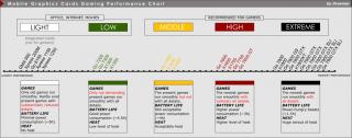
[thumbnail source : notebookreview.com's forum]
This post has been edited by lucifah: Dec 13 2006, 11:01 PM
Attached thumbnail(s)
 Quote
Quote


 Laptop having some of the limitation too...... if using high-end GC laptop display for playing games is very hot some more used alot of laptop battery energy too......


 0.0271sec
 0.45
0.45
 6 queries
 GZIP Disabled