

 Oct 29 2009, 10:29 AM, updated 16y ago

Background
The Cell concept was originally thought up by Sony Computer Entertainment inc. of Japan, for the PlayStation 3. The genesis of the idea was in 1999 when Sony’s Ken Kutaragi “Father of the PlayStation” was thinking about a computer which acted like Cells in a biological system. A patent was applied for listing Masakazu Suzuoki and Takeshi Yamazaki as the inventors in 2002 (the first version of this article covered this patent).
The architecture as it exists today was the work of three companies: Sony, Toshiba and IBM. Sony and Toshiba previously co-operated on the PlayStation 2 but this time the plan was more ambitious and went beyond chips for video games consoles. The aim was to build a new general purpose processor for a computer. With that in mind IBM was brought in as their expertise is in computer design.
“Though sold as a game console, what will in fact enter the home is a Cell-based computer.”- Ken Kutaragi
IBM also brought it’s chip design expertise and in this case used a very aggressive approach by producing a fully custom design - the chip’s circuitry was designed by hand instead of with automated tools, very few other companies use this approach. IBM also has the industry's leading silicon process which will be used in the manufacturing. Sony and Toshiba bring mass manufacturing capabilities and knowledge.
Each of the three companies produces different products and these have different needs of a CPU. Consumer electronics requires very power efficient systems, reliability and predictability. Computer systems on the other hand (sometimes) have multiple processors, and need to be compatible across different generations. The final Cell design incorporates features to satisfy all these needs.
To turn the ideas into a real product the the companies officially partnered in 2000 and set up a design centre in Austin, Texas in March 2001 with engineers from each of the three companies. Development was done in 10 centres around the globe by some 400 people.
The amount of money subsequently spent on this project is vast, two 65nm chip fabrication facilities are being built at billions each, Sony has paid IBM hundreds of millions to set up a production line in East Fishkill, New York. Then there's a few hundred million on development - all before a single chip rolls of the production lines.
Although it’s been primarily touted as the technology for the PlayStation 3, Cell is designed for much more. Sony and Toshiba, both being major electronics manufacturers buy in all manner of different components. One of the reasons for Cell's development is they want to save costs by building their own components. Next generation consumer technologies such as Blu-ray, HDTV, HD Camcorders and of course the PS3 will all require a very high level of computing power and they are going to need the chips to provide it. Cell will be used for all of these and more, IBM will also be using the chips in servers. The partners can also sell the chips to 3rd party manufacturers.
The Cell architecture is like nothing we have ever seen in commodity microprocessors, it is closer in design to multiprocessor vector supercomputers. The Cell developers have taken this kind of technology and for the first time are bringing it to your home. The aim is produce a low cost system with a massive increase in compute performance over existing systems. Putting such an architecture on a single chip is a huge, complex project, no other manufacturer appears to have even attempted to do anything this ambitious to date.
So, what is Cell Architecture?
Cell is an architecture for high performance distributed computing. It is comprised of hardware and software Cells, software Cells consist of data and programs (known as jobs or apulets), these are sent out to the hardware Cells where they are computed, the results are then returned.
This architecture is not fixed, if you have a computer, PS3 and HDTV which have Cell processors they can co-operate on problems. They've been talking about this sort of thing for years of course but the Cell is actually designed to do it. I for one quite like the idea of watching "Contact" on my TV while a PS3 sits in the background churning through SETI@home, actually this is rather unlikely as I’m not a gamer but you get the picture...
According to IBM the Cell performs 10x faster than existing CPUs on many applications. This may sound ludicrous but GPUs (Graphical Processors Units) already deliver similar or even higher sustained performance in many non-graphical applications. The technology in the Cell is similar to that in GPUs so such high performance is certainly well within the realm of possibilities. The big difference is though that Cell is a lot more general purpose so can be usable for a wider variety of tasks.
The Cell architecture can go further though, there's no reason why your system can't distribute software Cells over a network or even all over the world. The Cell is designed to fit into everything from (eventually) PDAs up to servers so you can make an ad-hoc Cell computer out of completely different systems.
Scaling is just one capability of the Cell architecture but the individual systems are going to be potent enough on their own. An individual Cell is one hell of a powerful processor, they have a theoretical computing capability of 256 GFLOPS (Billion Floating Point Operations per Second) at 4GHz. In the computing world quoted figures (bandwidth, processing, throughput) are often theoretical maximums and rarely if ever met in real life. Cell may be unusual in that given the right type of problem they may actually be able to get close to their maximum computational figure.
This isn’t by luck or fluke, it’s by design. The Cell’s hardware has been specifically designed to provide sufficient data to the computational elements to enable such performance. This is a rather different approach from the usual way which is to hide the slower parts of the system. All systems are limited by their slowest components, Cell was designed not to have any slow components!
Specifications
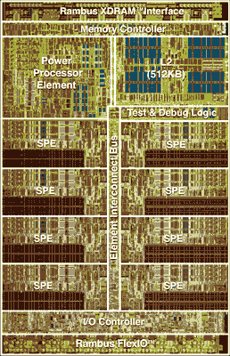
An individual hardware Cell is made up of a number of elements:
1. 1 Power Processor Element (PPE).
2. 8 Synergistic Processor Elements (SPEs).
3. Element Interconnect Bus (EIB).
4. Direct Memory Access Controller (DMAC).
5. 2 Rambus XDR memory controllers.
6. Rambus FlexIO (Input / Output) interface.

The final specifications haven't been given out yet but this is what we know so far:
7. Capable of running at speeds beyond 4 GHz.
8. Memory bandwidth: 25.6 GBytes per second.
9. I/O bandwidth: 76.8 GBytes per second.
10. 256 GFLOPS (Single precision at 4 GHz).
11. 256 GOPS (Integer at 4 GHz).
12. 25 GFLOPS (Double precision at 4 GHz).
13. 235 square mm.
14. 235 million transistors.
Power consumption has been estimated at 60 - 80 Watts at 4 GHz for the prototype but this could change in the production version.
Chip manufacturing is a complex process and the chips that appear at the end of the production line vary in capabilities and some have errors. While they can go higher, because of the vagaries of manufacturing, economics and heat dissipation the Cell which will be used in the PS3 is clocked at 3.2 GHz and will have only 7 SPEs. Cells with 6 SPEs will be used in consumer electronics.
The Power Processor Element (PPE)
The PPE is a conventional microprocessor core which sets up tasks for the SPEs to do. In a Cell based system the PPE will run the operating system and most of the applications but compute intensive parts of the OS and applications will be offloaded to the SPEs.
As an example lets say I was running an audio synthesiser application. The OS and most of the application would run on the PPE but the highly intensive audio generation and processing would be off-loaded to the SPEs.
The PPE is a 64 bit, "Power Architecture" processor with 512K cache. Power Architecture is a catch all term IBM have been using for a while to describe both PowerPC and POWER processors. This type of microprocessor is not used in PCs but compatible processors are found in Apple Macintosh systems. The PPE is capable of running POWER or PowerPC binaries.
While the PPE uses the PowerPC instruction set, it is not based on an existing design on the market today. That is to say, it is NOT based on the existing 970 / G5 or POWER processors. It is a completely different architecture so clock speed comparisons are completely meaningless.
The PPE is a dual issue, dual threaded, in-order processor. Unlike many modern processors the hardware architecture is an “old style” RISC design, i.e. the PPE has a relatively simple architecture. Most modern microprocessors devote a large amount of silicon to executing as many instructions as possible at once by executing them "out-of-order" (OOO). This type of design is widely used but it requiring hefty amounts of additional circuitry and consumes large amounts of power. With the PPE, IBM have not done this and have instead gone with a much simpler design which uses considerably less power than other PowerPC devices - even at higher clock rates.
This design will however have the downside of potentially having rather erratic performance on branch laden applications. Such a simple CPU needs the compiler to do a lot of the scheduling work that hardware usually does so a good compiler will be essential. That said, the Cell's high bandwidth memory and I/O subsystems and the PPE's high clock speed and dual threading capability may well make up for these potential performance deficiencies.
Some of the technology in the PPE has been derived from IBM's high end POWER series of CPUs, Like POWER5 the PPE has the ability to run 2 threads simultaneously. When one thread is stalled and is waiting for data the second thread can issue instructions keeping the instruction units busy. IBM's hypervisor technology is also used allowing the Cell to run multiple operating systems simultaneously. According to IBM the Cell can run a normal OS alongside a real time OS with both functioning correctly.
Another interesting point about the PPE is that it includes support for the VMX vector instructions, (also known as "AltiVec" or "Velocity Engine"). VMX can speed up anything from financial calculations to operating system functions though it (or its PC equivalents) don't appear to be that widely used currently. One company which does use VMX extensively is Apple who use it to accelerate functions in OS X, it would not have been a huge job for Apple to utilise the PPE in the Cell.
A lesser known feature which appears to be present is memory tags required by some of IBM's "big iron" operating systems. I don’t know the purpose of these tags (they are optional in power architecture) but the Cell is said to be capable of running OS/400 and this requires them. It is not confirmed these are present but if so it looks like IBM could have some interesting plans for the Cell which involve rather more than gaming...IBM’s Unix variant, AIX is also said to be running on Cell. (Note: none of this is confirmed).
The PPE is an interesting processor and it looks likely that similar cores will turn up in systems other than the Cell. The CPU cores used in the XBox360 while different, appear to be derived from the same original design.
As mentioned above the PPE has been simplified compared to other desktop processors, I discuss the reasons behind this and their implications in part 4.
A 4GHz PowerPC sounds like a pretty potent processor until you realise that the PPEs are really just used as controllers in the Cell - the real action is in the SPEs:
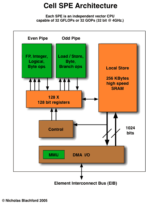
Synergistic Processor Elements (SPEs)
Each Cell contains 8 SPEs.
An SPE is a self contained vector processor which acts as an independent processor. They each contain 128 x 128 bit registers, there are also 4 (single precision) floating point units capable of 32 GigaFLOPS* and 4 Integer units capable of 32 GOPS (Billions of integer Operations per Second) at 4GHz. The SPEs also include a small 256 Kilobyte local store instead of a cache. According to IBM a single SPE (which is just 15 square millimetres and consumes less than 5 Watts at 4GHz) can perform as well as a top end (single core) desktop CPU given the right task.
*This is counting Multiply-Adds which count as 2 instructions, hence 4GHz x 4 x 2 = 32 GFLOPS.
32 X 8 SPEs = 256 GFLOPS
Like the PPE the SPEs are in-order processors and have no Out-Of-Order capabilities. This means that as with the PPE the compiler is very important. The SPEs do however have 128 registers and this gives plenty of room for the compiler to unroll loops and use other techniques which largely negate the need for OOO hardware.
Vector Processing
The SPEs are vector (or SIMD) processors. That is, they do multiple operations simultaneously with a single instruction. Vector computing has been used in supercomputers since the 1970s (the Cray 1 was one of the first to use the technique) and modern CPUs have media accelerators (e.g. MMX, SSE, VMX / AltiVec) which work on the same principle. Each SPE is capable of 4 X 32 bit operations per cycle (8 if you count multiply-adds). In order to take full advantage of the SPEs, the programs running will need to be "vectorised", this can be done in many application areas such as video, audio, 3D graphics, scientific calculations and can be used at least partially in many other areas.
Some compilers can “autovectorise” code, this involves analysing code for sections which can utilise a vector processor and needs no involvement from he developer. This can deliver considerable performance improvements and as such is an area of active research and development, v4.0 of the open source GCC compiler includes some of this functionality.
AltiVec?
The SPE's instruction set is similar to VMX / AltiVec but not identical. Some instructions have been removed and others added, the availability of 128 registers also makes a considerable difference in what is possible. Some changes are the addition of 64 bit floating point operations and program flow control operations as well as the removal of integer saturation rounding.
Another one of the differences is between the double and single precision capabilities. The double precision calculations are IEEE standard whereas the single precision are not. By not using IEEE standards the single precision calculations can be calculated faster, this feature appears to have been derived from the PS2 which did the same.
Despite these differences, according to IBM, by making some relatively minor changes and taking into account the SPE's local stores, software should compile to either an SPE or PowerPC (+ VMX) target. That said the binary code used is different so existing AltiVec binaries will not work.
Double Precision FLOPS
Double precision (64 bit) floating point data types are used when dealing with very large or small numbers or when you need to be very accurate. The first version of Cell supports these but the implementation shares the computation area of the single precision floating point units. Sharing these means the designers have saved a lot of room but there is a performance penalty, the first generation Cell can "only" do around 25 dual precision GFLOPS at 4 GHz. The first generation however are designed for the PS3 where high double precision operations are not necessary. IBM have alluded to the possibility that a later generation will include full speed dual precision floating point units from which you can expect a very sizeable performance boost.
SPE Local Stores
One way in which SPEs operate differently from conventional CPUs is that they lack a cache and instead use a “Local Store”. This potentially makes them (slightly) harder to program but they have been designed this way to reduce hardware complexity and increase performance. That said, if you use vector units and take account of the cache when you program a conventional CPU, developing optimised code for the SPE may actually be easier as you don’t need to worry about cache behaviour.
Conventional Cache
Conventional CPUs perform all their operations in registers which are directly read from or written to main memory. Operating directly on main memory is hundreds of times slower than using registers so caches (a fast on chip memory of sorts) are used to hide the effects of going to or from main memory. Caches work by storing part of the memory the processor is working on. If you are working on a 1/2 MB piece of data it is likely only a small fraction of this (perhaps a couple of thousand bytes) will be present in cache. There are kinds of cache design which can store more or even all the data but these are not used as they are too expensive, too slow or both.
If data being worked on is not present in the cache, the CPU stalls and has to wait for this data to be fetched. This essentially halts the processor for hundreds of cycles. According to the manufacturers, it is estimated that even high end server CPUs such as POWER, Itanium and PA-RISC (all with very large, very fast caches) spend anything up to 80% of their time waiting for memory.
Dual-core CPUs will become common soon and desktop versions have a cache per core. If either of the cores or other system components try to access the same memory address, the data in the cache may become out of date and thus needs updated (made coherent). Supporting this requires logic and takes time and in doing so this limits the speed that a conventional system can access memory and cache. The more processors there are in a system the more complex this problem becomes. Cache design in conventional CPUs speeds up memory access but compromises are required to make it work.
SPE Local Stores - No Cache?
To solve the complexity associated with cache design and to increase performance the Cell designers took the radical approach of not including any. Instead they used a series of 256 Kbyte “local stores”, there are 8 of these, 1 per SPE. Local stores are like cache in that they are an on-chip memory but the way they are constructed and act is completely different. They are in effect a second-level register file.
The SPEs operate on registers which are read from or written to the local stores. The local stores can access main memory in blocks of 1Kb minimum (16Kb maximum) but the SPEs cannot act directly on main memory (they can only move data to or from the local stores).
By not using a caching mechanism the designers have removed the need for a lot of the complexity which goes along with a cache and made it faster in the process. There is also no coherency mechanism directly connected to the local store and this simplifies things further.
This may sound like an inflexible system which will be complex to program but it’ll most likely be handled by a compiler with manual control used if you need to optimise.
This system will deliver data to the SPE registers at a phenomenal rate. 16 bytes (128 bits) can be moved per cycle to or from the local store giving 64 Gigabytes per second, interestingly this is precisely one register’s worth per cycle. Caches can deliver similar or even faster data rates but only in very short bursts (a couple of hundred cycles at best), the local stores can each deliver data at this rate continually for over ten thousand cycles without going to RAM.
One potential problem is that of “contention”. Data needs to be written to and from memory while data is also being transferred to or from the SPE’s registers and this leads to contention where both systems will fight over access slowing each other down. To get around this the external data transfers access the local memory 1024 bits at a time, in one cycle (equivalent to a transfer rate of 0.5 Terabytes per second!).
This is just moving data to and from buffers but moving so much in one go means that contention is kept to a minimum.
In order to operate anything close to their peak rate the SPEs need to be fed with data and by using a local store based design the Cell designers have ensured there is plenty of it close by and it can be read quickly. By not requiring coherency in the Local Stores, the number of SPEs can be increased easily. Scaling will be much easier than in systems with conventional caches.
Local Store V’s Cache
To go back to the example of an audio processing application, audio is processed in small blocks so to reduce any delay as the human auditory is highly sensitive to this. If the block of audio, the algorithm used and temporary blocks can fit into an SPE’s local store the block can be processed very, very fast as there are no memory accesses involved during processing and thus nothing to slow it down. Getting all the data into the cache in a conventional CPU will be difficult if not impossible due to the way caches work.
It is in applications like these that the Cell will perform at its best. The use of a local store architecture instead of a conventional cache ensures the data blocks can be hundreds or thousands of bytes long and they can all be guaranteed to be in the local store. This makes the Cell’s management of data fundamentally different from other CPUs.
The Cell has massive potential computing power. Other processors also have high potential processing capabilities but rarely achieve them. It is the ability of local stores to hold relatively large blocks of data that may allow Cells to get close to their maximum potential.
Local stores are not a new invention, in the early 1990s the AT&T DSP Commodore were planning on using in a never released Amiga included a “visible cache”. They go back further though, a local store type arrangement was used in the 1985 Cray 2 supercomputer.
Locking Cache
The PPE as a more conventional design does not have a local store but does include a feature called a “locking cache”. This stops data in parts of the cache being overwritten allowing them to act like a series of small local stores. This is used for streaming data into and out of the PPE or holding data close that is regularly needed. If the locked part acted like a normal cache the data being held could get flushed out to main memory forcing the PPE to stall while it was being retrieved, this could cause performance to plummet in some instances (a memory read can take hundreds of cycles).
Locking caches are common in embedded processors, Intel’s XScale and the XBox360’s CPUs include them as do modern G3 and G4s. They are not generally included in desktop processors due to their more general purpose nature. Using cache locking in a desktop environment could prove catastrophic for performance as applications working on data close to that locked would not be able to use the cache at all. It is possible to achieve similar results with clever programming tricks and this is a much better idea in a multitasking environment.
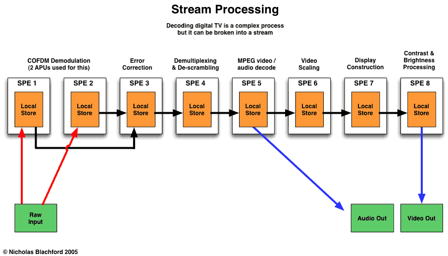
Steam Processing
A big difference in Cells from normal CPUs is the ability of the SPEs in a Cell to be chained together to act as a stream processor. A stream processor takes data and processes it in a series of steps.
A Cell processor can be set-up to perform streaming operations in a sequence with one or more SPEs working on each step. In order to do stream processing an SPE reads data from an input into it's local store, performs the processing step then stores the result into it's local store. The second SPE reads the output from the first SPE's local store and processes it and stores it in it's output area.
This sequence can use many SPEs and SPEs can access different blocks of memory depending on the application. If the computing power is not enough the SPEs in other Cells can also be used to form an even longer chain.
Stream processing does not generally require large memory bandwidth but Cell has it anyway and on top of this the internal interconnect system allows multiple communication streams between SPEs simultaneously so they don’t hold each other up.
So you think your PC is fast...
It is when the SPEs are working on compute heavy streaming applications that the Cell will be working hardest. It's in these applications that the Cell may get close to it's theoretical maximum performance and perform an order of magnitude more calculations per second than any desktop processor currently available.
On the other hand if the stream uses large amounts of bandwidth and the data blocks can fit into the local stores the performance difference might actually be bigger. Even if conventional CPUs are capable of processing, the data at the same rate the transfers between the CPUs will be held up while they wait for chip to chip transfers. The Cell’s internal interconnect system allows transfers running into hundreds of Gigabytes per second, chip to chip interconnects allows transfers in the low 10’s of Gigabytes per second.
While conventional processors have vector units on board (SSE or VMX / AltiVec) they are not dedicated vector processors. The vector processing capability is an add-on to the existing instruction sets and has to share the CPUs resources. The SPEs are dedicated high speed vector processors and with their own memory don't need to share anything other than the memory (and not even this much if the data can fit in the local stores). Add to this the fact there are 8 of them and you can see why their potential computational capacity is so large.
Such a large performance difference may sound completely ludicrous but it's not without precedent, in fact if you own a reasonably modern graphics card your existing system is already capable of similar processing feats:
"For example, the Nvidia GeForce 6800 Ultra, recently released, has been observed to reach 40 GFlops in fragment processing. In comparison, the theoretical peak performance of the Intel 3GHz Pentium4 using SSE instructions is only 6GFlops."
“GPUs are >10x faster than CPU for appropriate problems”
The 3D Graphics chips in computers have long been capable of very much higher performance than general purpose CPUs. Previously they were restricted to 3D graphics processing but since the addition of vertex and pixel shaders people have been using them for more general purpose tasks, this has not been without some difficulties but Shader 4.0 parts are expected to be even more general purpose than before.
Existing GPUs can already provide massive processing power when programmed properly but this is not exactly an easy task. The difference with the Cell is it will be cheaper, considerably easier to program and will be useable for a much wider class of problems.
The EIB and DMAC
The original patent application describes a DMAC (Direct Memory Access Controller) which controlled memory access for the SPEs / PPE (then known as the APUs and the PU) and connected everything with a 1024 bit bus. The original DMAC design also included the memory protection system.
The DMAC has changed considerably as the system evolved from the original design into the final product. The final version is quite different from the original but many parts still exist in one way or another. A DMAC still exists and controls memory access but it no longer controls memory protection. The 1024 bit interconnect bus was also replaced with a series of smaller ring busses called the EIB (Element Interconnect Bus).
The EIB consists of 4 x 16 byte rings which run at half the CPU clock speed and can allow up to 3 simultaneous transfers. The theoretical peak of the EIB is 96 bytes per cycle (384 Gigabytes per second) however, according to IBM only about two thirds of this is likely to be achieved in practice.
The original 1024 bit mentioned in the patent bus no longer connects the system together but it still exists in between the I/O buffer and the local stores. The memory protection was replaced completely by MMUs and moved into the SPEs.
It's clear to me that the DMAC and EIB combination is one of the most important parts of the Cell design, it doesn't do processing itself but has to contend with potentially hundreds of Gigabytes of data flowing through it at any one time to many different destinations as well as handling a queue of some 128 memory requests.
Memory and I/O
All the internal processing units need to be fed so a high speed memory and I/O system is an absolute necessity. For this purpose Sony and Toshiba licensed the high speed "Yellowstone" and "Redwood" technologies from Rambus, these are used in the the XDR RAM and FlexIO.
Both of these are interesting technologies not only for their raw speed but they have also been designed to simplify board layouts. Engineers spend a lot of time making sure wires on motherboards are all exactly the same length so signals are synchronised. FlexIO and XDR RAM both have a technology called "FlexPhase" which allow signals to come in at different times reducing the need for the wires to be exactly the same length, this will make life considerably easier for board designers working with the Cell.
As with everything else in the Cell architecture the memory system is designed for raw speed, it will have both low latency and very high bandwidth. As mentioned previously the SPEs access memory in blocks of 128 bytes. It’s not clear how the PPE accesses memory but 128 bytes happens to be a common cache line size so it may do the same.
The Cell will use high speed XDR RAM for memory. A Cell has a memory bandwidth of 25.6 Gigabytes per second which is considerably higher than any PC but necessary as the SPEs will eat as much memory bandwidth as they can get. Even given this the buses are not large (72 data pins in total), this is important as it keeps chip manufacturing costs down. The Cells runs it’s memory interface at 3.2 Gigabits per second per pin though memory in production now is already capable of higher speeds than this. XDR is designed to scale to 6.4 Gigabits per second so memory bandwidth has the potential to double.
Memory Capacity
The total memory that can be attached is variable as the XDR interface is configurable, Rambus’ site shows how 1GB can be connected. Theoretically an individual Cell can be attached to many Gigabytes of memory depending on density of the the RAM chips in use and this may involve using one pin per physical memory chip which reduces bandwidth.
SPEs may need to access memory from different Cells especially if a long stream is set up, thus the Cells also include a high speed interconnect. This consists of a set of 12 x 8 bit busses which run at 6.4 Gigabit / second per wire (76.8 Gigabytes per second total). The busses are directional with 7 going out and 5 going in.
The current systems allows 2 Cells to be connected glue-less (i.e. without additional chips). Connecting more Cells requires an additional chip. This is different from the patent as it specified 4 Cells could be directly connected and a further 4 could be connected via a switch.
IBM have announced a blade system made up of a series of dual Cell “workstations”. The system is rated at up to 16 TeraFlops, which will require 64 Cells.
Memory Management Units
Memory management is used to stop programs interfering with each other and to move data to disc when it is not in use.
The original Cell patent had two mechanisms for memory protection one of which was very simple and very fast while the second was very complex and slow. These have been replaced by a more conventional system used when accessing main memory.
While there is no protection or coherency mechanisms used within the local stores (again for simplicity and speed), the PPE and SPEs do contain Memory Management Units (MMUs) used when accessing memory or other SPEs’ local stores.
These act just like a conventional multiprocessor system and as such are much more sophisticated than the method described in the original patent. Multiprocessor systems is an area IBM are long experienced in so this change appears to have come from them. While this may be slower than the fast system in the patent the difference in reality is likely to be insignificant.
Processing Concrete
The Cell architecture goes against the grain in many areas but in one area it has gone in the complete opposite direction to the rest of the technology industry.
Operating systems started as a rudimentary way for programs to talk to hardware without developers having to write their own drivers every time. As time went on operating systems have evolved and taken on a wide variety of complex tasks, one way it has done this is by abstracting more and more away from the hardware.
Object oriented programming goes further and abstracts individual parts of programs away from each other. This has evolved into Java like technologies which provide their own environment thus abstracting the application away from the individual operating system, many other languages including C#, Perl and Python do the same. Web technologies do the same thing, the platform which is serving you with this page is completely irrelevant, as is the platform viewing it. When writing this I did not have to make a Windows or Mac specific version of the HTML, the underlying hardware, OSs and web browsers are completely abstracted away.
If there is a law in computing, abstraction is it, it is an essential piece of today's computing technology, much of what we do would not be possible without it.
Cell however, has gone against the grain and actually removed a level of abstraction. The programming model for the Cell will be concrete, when you program an SPE you will be programming what is in the SPE itself, not some abstraction. You will be "hitting the hardware" so to speak. The SPEs programming model will include 256K of local store and 128 registers, the SPE itself will include 128 registers and 256K of local store, no less, no more.
In modern x86 or PowerPC / POWER designs the number of registers present is different from the programming model, in the Transmeta CPUs it’s not only the registers, the entire internal architecture is different from what you are programming.
While this may sound like sacrilege and there are reasons why it is a bad idea in general there is one big advantage: Performance. Every abstraction layer you add adds computations and not by some small measure, an abstraction can decrease performance by a factor of ten fold. Consider that in any modern system there are multiple abstraction layers on top of one another and you'll begin to see why a 50MHz 486 may of seemed fast years ago but runs like a small dog these days, you need a more modern processor to deal with the subsequently added abstractions.
The big disadvantage of removing abstractions is it will add complexity for the developer and it limits how much the hardware designers can change the system. The latter has always been important and is essentially THE reason for abstraction but if you've noticed modern processors haven't really changed much in years. AMD64 is a big improvement over the Athlon but the overall architecture is actually very similar, Intel’s Pentium-M traces it’s linage right the way back to the Pentium Pro. The new dual core devices from AMD, Intel and IBM have not changed the internal architecture at all.
The Cell designers obviously don't expect their architecture to change much either so have chosen to set it in stone from the beginning. That said there is some flexibility in the system so it can still evolve over time.
The Cell approach does give some of the benefits of abstraction though. Java has achieved cross platform compatibility by abstracting the OS and hardware away, it provides a "virtual machine" which is the same across all platforms, the underlying hardware and OS can change but the virtual machine does not.
Cell does this but in a completely different way. Java provides a software based "virtual machine" which is the same on all platforms, Cell provides a machine as well - but they do it in hardware, the equivalent of Java's virtual machine is the Cells physical hardware. If I was to write code for SPEs on OS X the exact same Cell code would run on Windows, Linux or Zeta because in all cases it is the hardware Cells which execute it.
This does not however mean you have to program the Cells in assembly, Cells have compilers just like everything else. Java provides a “machine” but you don't program it directly either.
By actually providing 128 real registers (32 for the PPE) and 256K of local store they have made life more difficult for compiler writers but in some respects they’ve also made it easier, it’ll be a lot easier to figure out what’s going on and thus optimise for. There’s no need to try and figure out what will or will not be put in rename registers since these don’t exist.
Hard Real Time Processing
Some stream processing needs to be timed exactly and this has also been considered in the design to allow "hard" real time data processing. An "absolute timer" is used to ensure a processing operation falls within a specified time limit. This is useful on it's own but also ensures compatibility with faster next generation Cells since the timer is independent of the processing itself.
Hard real time processing is usually controlled by specialist operating systems such as QNX which are specially designed for it. Cell's hardware support for it means pretty much any OS will be able to support it to some degree or another. This will not however magically provide everything an RT OS provides (they are designed for bomb proof reliability) so things like QNX won’t be going away anytime soon from safety critical areas.
An interesting aspect of the Cell is that it includes IBMs virtualisation technology, this allow multiple operating systems to run simultaneously. This ability can be combined with the real time capability allowing a real time OS to run alongside a non-real time OS. Such an ability could be used in industrial equipment allowing a real time OS to perform the critical functions while a secondary non real time OS can act as a monitoring, display and control system. This could lead to all sorts of interesting possibilities of hybrid operating systems - how about Linux doing the GUI and I/O while QNX handles the critical stuff?
To DRM or not to DRM?
Some will no doubt be turned off by the fact that DRM (Digital Rights Management) is said to be built into the Cell hardware. Sony is a media company and like the rest of the industry that arm of the company are no doubt pushing for DRM type solutions. It must also be noted that the Cell is destined for HDTV and BluRay / HD-DVD systems. Like it or not, all high definition recorded content is going to be very strictly controlled by DRM so Sony have to add this capability otherwise they would be effectively locking themselves out of a large chunk of their target market. Hardware DRM is no magic bullet however, hardware systems have been broken before - including Set Top Boxes and even IBM's crypto hardware for their mainframes.
But is it really DRM?
While the system is taken to mean DRM I don't believe there is a specific scheme designed in, rather I think it may be more accurate to say the system has "hardware security" facilities. Essentially there’s a protection mechanism which can be used for DRM, but you could equally use it to protect your on-line banking.
The system enables an SPE to lock most of it’s local store for it's own use only. When this is done nothing else can access that memory. In this case nothing really means nothing, neither the OS or even the Hypervisor can access this memory while it is locked, only a small portion of the store remains unlocked so the SPE can still communicate with the rest of the system.
To give an example of how this could be useful, it could be used to address a perceived security weakness of the old WAP (Wireless Application protocol) system - think internet for mobile phones (note: I don't know current versions of the system so I'm referring to what they did in early versions). Originally the phones didn't have enough computing power to use the web's encryption system so a different system was used. Unfortunately this meant that the data would have to be decrypted from the web system then then re-encrypted into the new WAP system, this poses an immediate security problem. If a hacker could get into the system and gain root access they may be able to monitor the data when it was decrypted.
Cell could solve such a problem as the decryption and re-encryption could be done in a protected memory segment. Even if a hacker could get into the system getting root access would not help, even root cannot access that memory. Even if they were to get into hypervisor space they still couldn’t access the data, nothing gets in when it’s protected.
I doubt this system is still used by WAP gateways but if it is I’d expect WAP gateway manufacturers to suddenly become interested in Cell processors...
No details of how the system works have been released, I doubt if any system can be made un-hackable, but it doesn't seem like a direct attack would work in this case.
Other Options And The Future
There are plans for future technology in the Cell architecture. Optical interconnects appear to be planned, it's doubtful that this will appear anytime in the near future but clearly the designers are planning for the day when copper wires hit their limit (thought to be around 10GHz). Optical connections are quite rare and expensive at the moment but they look like they will become more common soon.
The design of Cells is not entirely set in stone, there can be variable numbers of SPEs and the SPEs themselves can include more floating point or integer calculation units. In some cases SPEs can be removed and other things such as I/O units or graphics processor placed in their place. Nvidia are proving the graphics hardware for the PS3 so this may be done within a modified Cell at some point.
As Moore's law moves forward and we get yet more transistors per chip I've no doubt the designers will take advantage of this. The idea of having 4 Cells per chip is mentioned in the patent but this isn’t likely to happen for 3-4 years yet as they are too big to fit on a single reasonably priced chip right now...
The first version of the Cell has high double precision floating point performance but it could be higher and I expect a future version to boost it significantly, possibly by as much as 5x.
This post has been edited by Joey Christensen: Oct 29 2009, 01:12 PM
 Quote
Quote


 0.0213sec
 0.45
0.45
 5 queries
 GZIP Disabled